MegaSquirt DB37 Connector & DB9 Serial Schematic with U6 Voltage Test Points
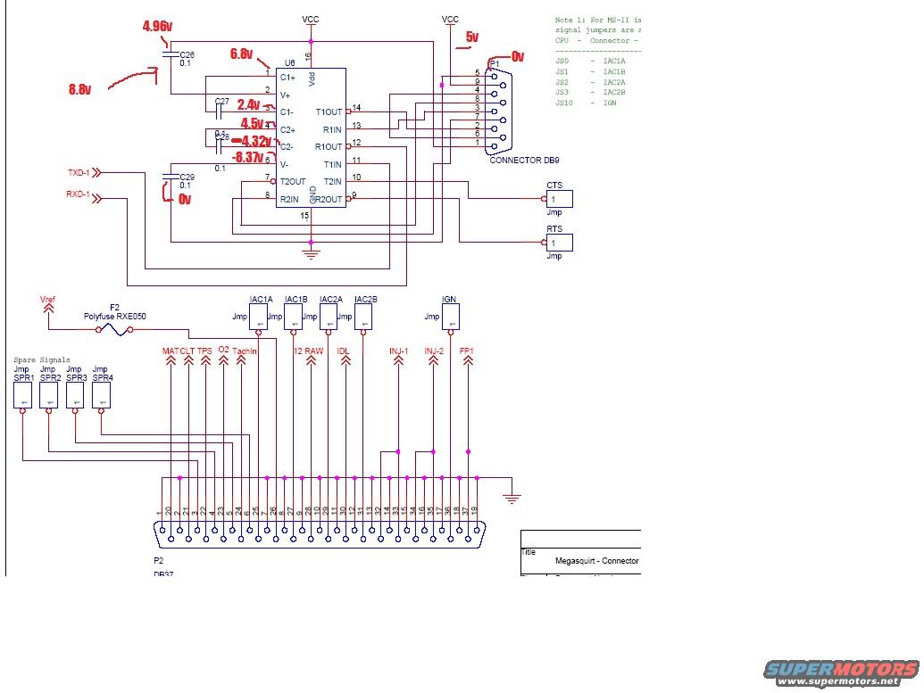
Reference · 1993-1997 ProbeAll 25 schematics
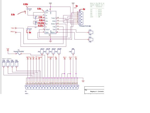
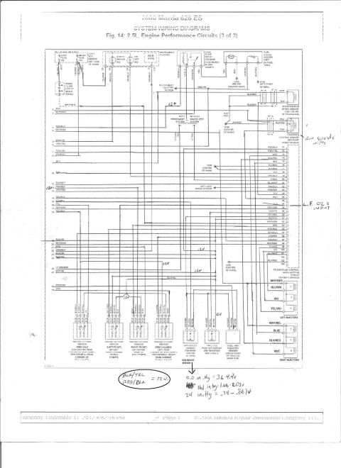
Megasquirt ECU connector schematic showing the DB9 serial interface, MAX232, input signal jumpers and the DB37 main connector pinout.
Part of 1993-1997 Ford Probe Schematics
This document is a page from a MegaSquirt DIY engine management (EFI controller) schematic, specifically the "Megasquirt - Connector" sheet. It shows the serial communications circuit built around U6 (a 16-pin RS-232 level converter with C1+/C1-/C2+/C2- charge-pump capacitors C26-C29, all 0.1 µF) connecting TXD-1 and RXD-1 to a DB9 connector (P1), with CTS and RTS jumper positions. Handwritten red voltage measurements have been added at various points on the charge-pump circuit (4.96v, 8.8v, 6.8v, 2.4v, 4.5v, -4.32v, -8.37v, 0v, 5v), suggesting the sheet was used to diagnose a serial communications or U6 chip fault. The lower half shows the main DB37 connector (P2) with its 37 numbered pins and the signals routed to it: MAT, CLT, TPS, O2, TachIn, 12 RAW, IDL, INJ-1, INJ-2, FP1, plus IAC1A/IAC1B/IAC2A/IAC2B and IGN jumpers, four spare signal jumpers (SPR1-SPR4), Vref, and polyfuse F2 (RXE050). A partial note explains that for MS-II certain CPU-to-connector signal jumpers are used: JS0-IAC1A, JS1-IAC1B, JS2-IAC2A, JS3-IAC2B, JS10-IGN. Useful for troubleshooting MegaSquirt serial comms and DB37 wiring.
Is this accurate? Sign in to help verify it.
Frequently asked questions
- What jumper settings does the note list for MS-II?
- The note lists CPU-to-connector jumpers: JS0 - IAC1A, JS1 - IAC1B, JS2 - IAC2A, JS3 - IAC2B, and JS10 - IGN.
- What signals go to the DB37 connector (P2) on this schematic?
- MAT, CLT, TPS, O2, TachIn, 12 RAW, IDL, INJ-1, INJ-2, FP1, plus IAC1A/IAC1B/IAC2A/IAC2B and IGN jumper outputs, Vref through polyfuse F2, and spare signals SPR1-SPR4.
- What are the capacitor values around U6?
- C26, C27, C28, and C29 are all 0.1 (µF) charge-pump/decoupling capacitors around the U6 serial level-converter IC.
- What voltages were measured on the U6 serial circuit?
- Handwritten measurements show 4.96v at C26, 8.8v and 6.8v on the V+ side, 2.4v and 4.5v at the C2 pins, -4.32v and -8.37v on the V- side, 0v at C29, 5v at VCC, and 0v at the DB9 connector.
- What fuse protects the Vref line?
- F2, a Polyfuse RXE050, is in series with the Vref line.
No comments yet.