Megasquirt MSII Power Supply Schematic - LM2937ET-5.0 5V Regulator & CPU Clock

Reference · 1993-1997 ProbeAll 25 schematics
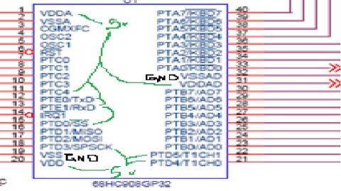
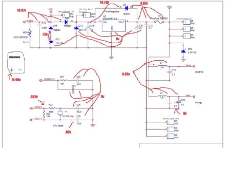
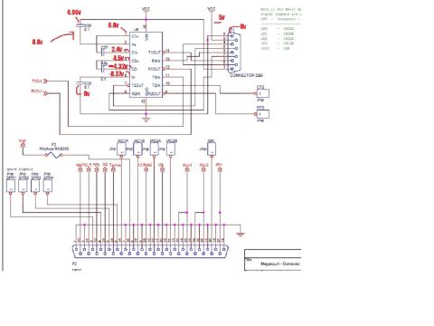
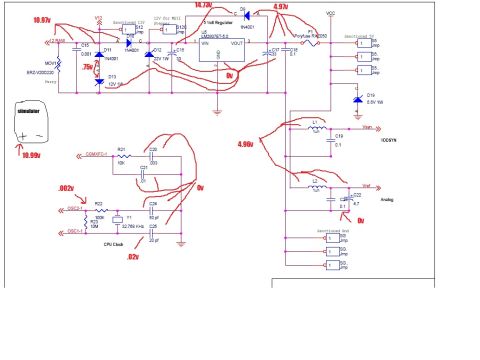
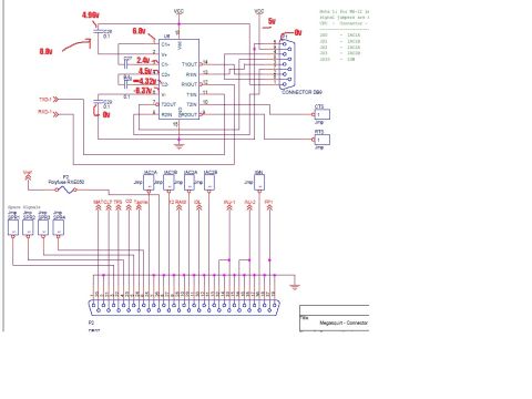
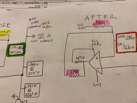
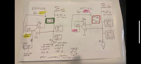
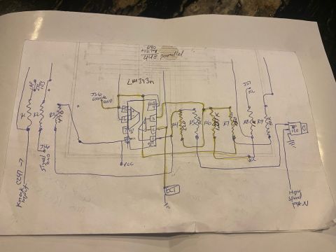
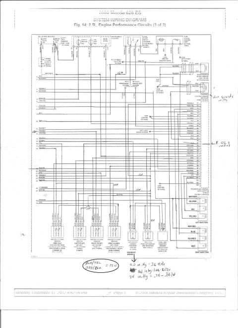
Megasquirt power-supply and voltage-regulator schematic annotated by hand with measured voltages at the regulator, CPU clock and rails.
Part of 1993-1997 Ford Probe Schematics
This document is a power supply schematic page (apparently from a Megasquirt-style engine controller board) with handwritten troubleshooting voltage measurements marked in red. The printed circuit shows a 12V raw input protected by MOV1 (ERZ-V20D220), diodes D10/D11 (1N4001), zeners D12 (22V 1W) and D13 (12V 1W), feeding a 5-volt regulator U5 (LM2937ET-5.0) with filter capacitors C16/C17 (33) and C18 (0.1). Output VCC passes through polyfuse F1 (RXE050) to "Sanctioned 5V" jumper positions, protected by zener D19 (5.6V 1W). LC filters L1/C19 and L2/C22/C23 derive Vsyn (VDDSYN) and Vref (Analog) rails. A CPU clock section shows crystal Y1 (32.768 KHz) with R21-R23, C20/C21, and load caps C24 (50 pf) and C25 (20 pf), plus nets CGMXFC-1, OSC1-1, OSC2-1. Jumper blocks are labeled Sanctioned 12V, 12V for MSII Stepper, Sanctioned 5V, and Sanctioned Gnd. Handwritten annotations record measured voltages at test points: 10.97v and 10.99v (input/stimulator), 14.73v, 4.97v and 4.96v (5V rails).75v.002v.02v, and several 0v points, useful for diagnosing a failed regulator or supply fault on the board.
Is this accurate? Sign in to help verify it.
Frequently asked questions
- What voltage regulator is used in this power supply schematic?
- U5, an LM2937ET-5.0 5-volt regulator, with VIN on pin 1, VOUT on pin 3, and GND on pin 2, marked "5 Volt Regulator".
- What protection components are on the 12V raw input?
- MOV1 (ERZ-V20D220), diodes D10 and D11 (both 1N4001), zener D13 (12V 1W), zener D12 (22V 1W), capacitor C15 (0.001), and polyfuse F1 (RXE050) on the 5V output. D19 is a 5.6V 1W zener on VCC.
- What crystal frequency is used for the CPU clock?
- Y1 is a 32.768 KHz crystal with load capacitors C24 (50 pf) and C25 (20 pf), plus R22 (100K) and R23 (10M), connected to OSC1-1 and OSC2-1.
- What voltages were measured on the board according to the handwritten notes?
- Input measurements of 10.97v and 10.99v (from a device sketched as a "stimulator"), 14.73v before D9, 4.97v and 4.96v on the 5V/Vsyn rails, .75v at D13, and low readings of .002v, .02v, and 0v at several points.
- How are the Vsyn and Vref rails generated?
- Vsyn (VDDSYN) comes from VCC through L1 (1uh) with C19 (0.1); Vref (Analog) comes through L2 (1uh) with C23 (0.1) and C22 (4.7).


No comments yet.