68HC908GP32 Microcontroller Pinout with 5V & GND Annotations - Ford Probe Schematic
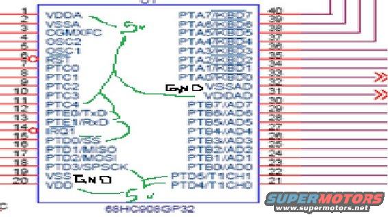
Schematic detail of a 68HC908GP32 microcontroller showing labeled pin functions and hand-drawn signal/ground connections.
This document is a cropped schematic excerpt showing the complete 40-pin pinout of a Motorola/Freescale 68HC908GP32 microcontroller, labeled U1. All 40 pins are shown with their signal names: power and oscillator pins (VDDA, VSSA, CGMXFC, OSC2, OSC1, RST, VSS, VDD, VSSAD, VDDAD), port C pins (PTC0–PTC4), serial pins (PTE0/TxD, PTE1/RxD), interrupt (IRQ1), SPI pins (PTD0/SS, PTD1/MISO, PTD2/MOSI, PTD3/SPSCK), keyboard-interrupt port A pins (PTA0/KBD0 through PTA7/KBD7), analog/port B pins (PTB0/AD0 through PTB7/AD7), and timer channel pins (PTD4/T1CH0, PTD6/T1CH1). Hand-drawn green annotations identify the chip's operating voltages: "5v" is marked at pin 1 (VDDA) and pin 20 (VDD), while "GND" is marked at pin 19 (VSS) and pin 32 (VSSAD), matching the file name "chip voltage.jpg." Red arrow markers highlight pins 31 (VDDAD) and 32 (VSSAD). A reader can learn the pin numbering, signal assignments, and where supply voltage and ground connect on this microcontroller, which appears to be part of a larger schematic (likely related to the instrument cluster or ECU electronics documents in the same album). No vehicle year, make, or model is stated on the document itself.
Is this accurate? Sign in to help verify it.
Frequently asked questions
- What chip is shown in this pinout diagram?
- A 68HC908GP32 microcontroller, designated U1, shown in a 40-pin package with all pin labels.
- Which pins on the 68HC908GP32 receive 5 volts according to the annotations?
- Handwritten "5v" annotations point to pin 1 (VDDA) and pin 20 (VDD).
- Which pins are marked as GND on this diagram?
- Handwritten "GND" callouts point to pin 19 (VSS) and pin 32 (VSSAD).
- Where are the keyboard interrupt pins (KBD0–KBD7) located?
- On the right side of the chip: pins 33 through 40, labeled PTA0/KBD0 up through PTA7/KBD7.
- Which pins carry the SPI signals?
- Pins 15–18 on the left side: PTD0/SS, PTD1/MISO, PTD2/MOSI, and PTD3/SPSCK.
Comments
More from this build

No comments yet.